什么是射频无源集成芯片IPD
What is RF Integrated Passive Device (IPD) Chip
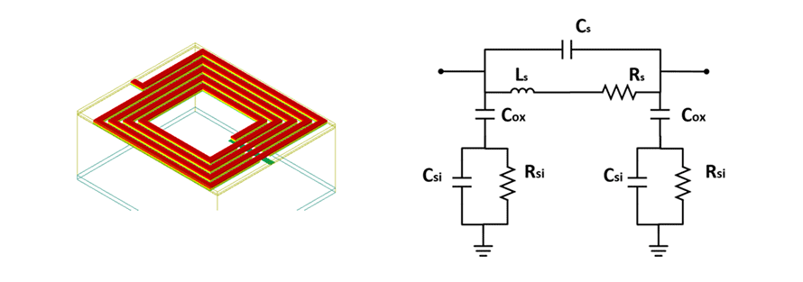
射频无源集成芯片(IPD)是一种基于晶圆制程的射频集成无源器件技术,其本质是基于高阻硅、砷化镓以及玻璃等绝缘介质的半导体无源器件集成技术。高加工精度,高良率,成熟稳定的先进晶圆制程使得射频IPD芯片具有众多优点:
RF integrated passive device (IPD) is a chip fabricated using wafer processes to integrate RF passive components altogether. The IPD technology is essentially a semiconductor integration technology based on high-resistance silicon, gallium arsenide, glass and other insulating substrates.With advanced highly accurate, high yield, mature and stable wafer manufacturing processes, RF IPD chips have many advantages:
- 小尺寸
- 低成本
- 易于集成
- 高一致性
- 灵活的设计方法和封装形式
- Small Size
- Low Cost
- Easy to Integrate
- High Uniformity
- Flexible Design and Packaging Approaches
作为一项实现小型化低成本无源器件的重要技术,IPD满足了当前各种无线应用场景对射频前端功能不断增加,集成度不断提高的需求,应用在各种无源器件,包括滤波器,双工器,巴伦,耦合器,功分器等。
As an important technology to achieve miniaturization and low-cost passive devices, the IPD technology meets demands of growing functions and increasing integration for RF front-end modules in various wireless applications, and can be employed to design a wide spectrum of passive devices, including filters, duplexers, baluns, couplers, power dividers, etc.
更小的尺寸、更薄的厚度、更高的集成度以及更低的量产成本使得IPD能够帮助面对物联网,手持和可穿戴设备等对射频前端小型化提出的挑战。
Smaller size, thinner thickness, higher integration, and lower costs in mass production enable IPD chips to circumvent miniaturization challenges of RF front-end modules in the internet of things, handhelds, wearables, etc.
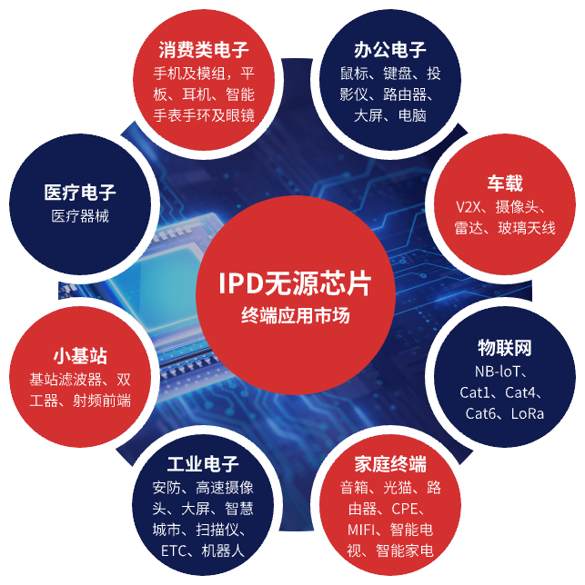
IPD集成芯片应用市场
IPD Market
IPD芯片在PCB模组中的应用
IPD Chips in PCB Modules
传统无源器件
Discrete Passive Components on PCB

离散SMD解决方案
SMD Technology


集成无源器件(IPD)技术
Integrated Passive Devices (IPDs)
IPD解决方案
IPD Technology
几十个无源器件用一个IPD芯片替代,不仅物料供应更为简单,需要的焊点也更少,电路变得简单,可靠性也会提高。
Dozens of passive components on PCB can be replaced by a single IPD chip, which not only simplifies the supply chain management, but also reduces the number of solder joints, and thus resulting in more reliable and simpler circuit module.
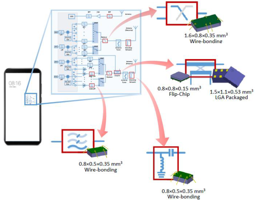
IPD芯片在4G/5G手机终端中的应用
IPD Chips in 4G/5G Mobile Phone Terminals

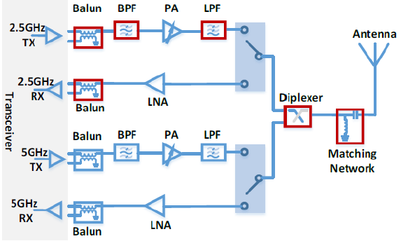
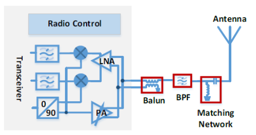
IPD芯片在无线连接射频前端中的应用
IPD Chips in RF Transceivers
典型的路由器射频前端中IPD芯片应用
Typical Scenario of IPD Chips in Router
典型的蓝牙器件射频前端中IPD芯片应用
Typical Scenario of IPD Chips in Bluetooth
IPD芯片在系统级封装(SiP)中的应用
IPD Chips in System-in-Package (SiP)

设计服务内容
Design Services
-
1.法动科技拥有自主开发的针对射频集成无源器件(IPD)芯片设计的全波仿真设计平台及优化工具,为客户开发相关工艺的PDK库和参数模型。
1.The in-house proprietary RF EDA platform can greatly speedup design and optimization of RF IPD chips, and readily develop models and PDK libraries under the targeted processes for customers.
-
2.开发一系列具有市场竞争力的通用型射频集成无源器件(IPD)芯片产品。
2.A series of general-purpose RF IPD chips can be selected off-the-shelf with market competitiveness.
-
3.开发基于客户需求的定制化射频集成无源器件(IPD)芯片产品以及相关各种封装形式。
3.Provide customized designs of RF IPD chips and related packaging based on customer's specifications.
设计服务优势
Our Advantages
-
1.法动科技拥有自主开发的针对集成无源芯片(IPD)芯片设计的全波仿真工具和平台,并且已开发出IPD芯片一次流片设计成功的成熟设计流程,可实现快速定制化的IPD设计,并且可将更多芯片内核集成(SIP),实现更高的芯片集成度。
1.In additional to the in-house proprietary RF EDA platform, a verified design flow for RF IPD chips has been developed, which offers one-time design success for rapid customized RF IPD designs. In addition, System-in-Chip (SiP) solution is also available for integrating multiple chips in a single package to achieve higher integration.
-
2.拥有电磁领域专业设计团队,拥有完善的IPD设计流程和工艺支持,并研发出多款IPD芯片采用新颖拓扑结构,在IPD芯片小型化,宽带化,降低插入插损,高带外抑制等方面开发出若干独创技术,并成功获得30余项相关技术专利授权。
2.We have a strongly experienced and highly professional in-house team, which is particularly specialized in electromagnetic designs. Moreover, we have developed a verified RF IPD design flow with close collaborations with foundries on the process supports, and successfully designed a number of RF IPD chips using novel topologies. Finally, we have more than 30 innovative patents that cover IPD miniaturization, broadband applications, insertion loss reduction, improvement of out-of-band suppression, etc.
-
3.法动科技已成功流片多款经过测试验证的高质量IPD专利产品,其性能优于市场同类产品的集成无源芯片,包括多款5G/Wifi频段滤波器、巴伦、耦合器、功分器等。
3.We have successfully streamed a number of high-quality patented RF IPD products that have been fully tested and verified, and their performances are better than the similar RF IPD products in the market, including 5G/Wi-Fi filters, Balun, couplers, power dividers, etc.
-
4.法动公司与各个芯片代工公司具有良好的长期合作关系(包括为各主流芯片代工开发基于其工艺库的PDK),可以保证相关芯片的产能交付以及芯片成本控制。
4.The company has established a very close long-term collaborations with various foundries (including developments of PDK libraries for the foundries), which can assure us the capacity of mass production with well controlled fabrication cost.
|
Part Number
|
Part Type
|
Wireless Technology
|
Pass Band(MHz)
|
Insertion Loss (dB Max)
|
Return Loss(dB)
|
Out of Band Rejection (dB)
|
Dimensions (mm)
|
Package
|
Spec Sheet
|
|---|---|---|---|---|---|---|---|---|---|
|
FDCD5GBPF001
|
Band Pass Filter
|
5G NR
|
3300-4200
|
1.55
|
15
|
45@1920-1980MHz
|
1.0×0.5×0.3
|
WLCSP
|
|
|
FDCD5GBPF002
|
Band Pass Filter
|
5G NR
|
3300-4200
|
1.7
|
18
|
30@5150-5925MHz
|
1.0×0.5×0.3
|
WLCSP
|
|
|
FDCD5GBPF003
|
Band Pass Filter
|
5G NR
|
3300-4200
|
0.8
|
22
|
20@2400-2480MHz
|
1.2××0.5×0.3
|
WLCSP
|
|
|
FDCD5GBPF004
|
Band Pass Filter
|
5G NR
|
3300-4200
|
1.8
|
18
|
45@1710-1785MHz
|
1.0×0.5×0.3
|
WLCSP
|
|
|
FDCDWFDUP001
|
Diplexer
|
Wifi
|
2.4-2.496GHz
&4.95-5.9GHz |
0.6dB@2400~2496MHz
1.0dB@4900~5950MHz |
18
|
26dB @30-2700 MHz
27dB @4900-5950 MHz |
1.6×0.8×0.3
|
WLCSP
|
|
|
FDCDW6DUP002
|
Diplexer
|
Wifi6
|
2.4-2.5GHz
&5.15-7.125GHz |
0.65dB@2400~2500MHz
1.5dB@5150~7125MHz |
18
|
24dB @4800-5000 MHz
27dB @5150-7125 MHz |
1.6×0.8×0.3
|
WLCSP
|
|
|
FDCD4GDUF003
|
Diplexer
|
3G/4G
|
0.699~0.960GHz
&1.71~2.69GHz |
0.65dBmax@0.699~0.960GHz
0.64dBmax@1.71~2.69 GHz |
16
|
20dB@0.699-0.915GHz
20dB@1.71-2.69GHz |
1.6×0.8×0.3
|
WLCSP
|
|
|
FDDIV001
|
Power Divider
|
LTE, WLAN / WiMax
|
800-1000
|
0.45
|
20
|
N/A
|
1.0×0.5×0.75
|
Die
|
|
|
FDBAL001
|
Balun
|
5G NR
|
2800-6000
|
1.2
|
15
|
N/A
|
1.0×0.9×0.75
|
Die
|
什么是射频无源器件和天线设计
What is RF Passive Device or Antenna
射频(Radio Frequency, RF)无源器件是指在射频电路中不需要外部能量输入的器件,通常不包含源,如放大器和振荡器。这些器件在射频和微波系统中发挥关键作用,用于处理、传输和控制射频信号。
Radio frequency (RF) passive device is an RF device that does not require a power supply and typically does not contain a power source (i.e., amplifier or oscillator). The RF passive devices play a critical role in RF and microwave systems to process, transmit, and control RF signals.
天线是一种用于发送和接收电磁波的设备,广泛应用于通信、雷达、导航、广播、卫星通信、移动通信等领域。天线的设计主要取决于其应用领域和工作频段。天线的类型可分为几大类,主要包括全向天线,定向天线,螺旋天线,阵列天线等。
Antenna is a device for transmitting and receiving electromagnetic waves, which is widely used in wireless communication, radar, navigation, broadcasting, satellite communication, mobile communication and other fields. The design of antennas mainly depends on its application field and operating frequency band. The type of antenna can be classified into several categories, mainly including omnidirectional antenna, directional antenna, spiral antenna, antenna array and so on.
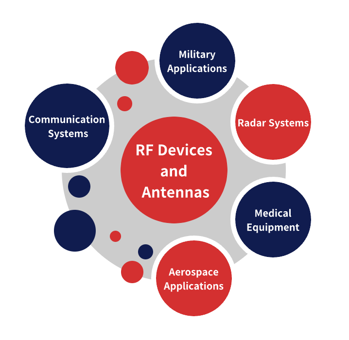
射频无源器件和天线设计应用场景
RF Passive Device and Antenna Market
射频无源器件主要应用于无线通信系统基站建设和室内分布系统中。特别是在建筑物内的无线信号室内分布覆盖中应用种类繁多,数量庞大。射频无源器件在基站建设和室内分布工程中起到连接或分配射频信号的作用。室内分布系统是将基站发射的信号通过射频无源器件进行连接或分路,经由馈线分散到各覆盖点天线处,从而达到室内无线信号连续良好的覆盖。
RF passive devices are mainly used in wireless communication base stations, indoor wireless systems, and wireless terminal equipment. Particularly, there are large quantities of applications for indoor coverage of wireless signals in buildings. RF passive devices process, switch, and control RF signals among wireless communication base stations, indoor wireless systems, and wireless terminal equipment.
天线的设计应用场景广泛,涵盖了许多不同的领域和应用。以下是一些常见的天线设计应用场景:移动通信,卫星通信,WLAN和Wi-Fi,雷达系统,射频识别(RFID),和电子导航。这些只是天线应用的一小部分示例,随着科技的发展和新兴应用的涌现,天线设计在各个领域都有着重要的作用。设计者需要根据具体的应用需求和环境条件来选择合适的天线类型和特性。
Antennas have a wide range of application scenarios, covering various fields and applications, such as mobile communications, satellite communications, WLAN and Wi-Fi, radar systems, radio frequency identification (RFID), and electronic navigation. With advancement of technology, novel antennas play important roles in various fields. Designers need to choose the appropriate antenna type and characteristics according to the specific application requirements and environmental conditions.
设计服务内容
Design Services
射频无源器件和天线的设计需要使用仿真工具对设计进行建模和优化,选择适用于射频无源器件的材料,并进行相应的特性分析,以确保其在特定环境下的稳定性和可靠性使其性能满足预期要求。
The design of RF passives and antennas requires the use of EDA design tools to model and optimize the design, and select the appropriate materials and characterize them accordingly to ensure stability and reliability of RF passives and antennas to meet the performance requirements under the given operating environments.
法动拥有突出的射频无源器件和天线设计能力,可提供的全方位、全专业的高水平设计服务,其中包括各种类型的天线、滤波器、巴伦等无源器件的设计。
We have outstanding in-house design capabilities of RF passives and antennas, and can provide a full range of excellent professional design services, including designs of various types of antennas, filters, baluns, and other passive components.
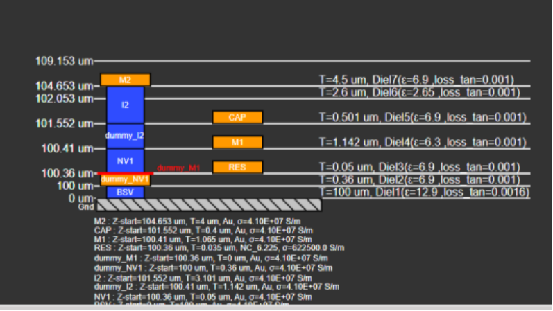
无源器件LTCC滤波器
LTCC Filters
设计LTCC滤波器产品具有尺寸小、低插损和高带外抑制等优势。
Our designs of LTCC filters have merits of small size, low insertion loss, and high out-of-band rejection.
无源器件LTCC巴伦
LTCC Baluns
法动所设计LTCC巴伦产品采用多层螺旋耦合线,耦合系数高,结构紧凑。同时内嵌入匹配电路,使其具有更宽的通带。
Our designs of LTCC baluns adopt a multi-layer spiral coupling line, with a high coupling coefficient and compact structure. At the same time, the matching circuit is integrated within the designs, leading to a wider passband.
天线AiP双极化天线
Dual-Polarized AiP Antennas
法动所设计AiP天线具有低交叉极化、高增益、低互耦 、宽工作带宽和大角度扫描等优势。
Our designs of dual-polarized AiP antennas have merits of low cross-polarization, high gain, low coupling, wide bandwidth, and large scanning angle.

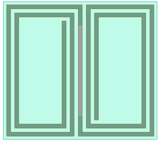
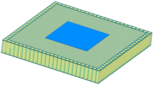
LTCC滤波器平面图
Top View of LTCC Filters

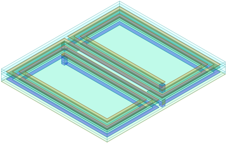
LTCC滤波器3D图
3D View of LTCC Filters
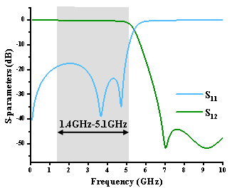
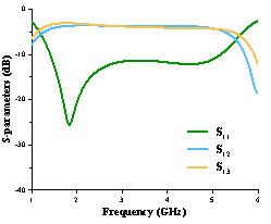
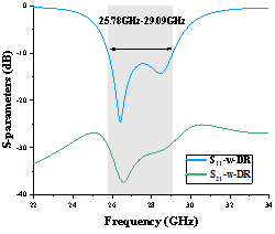
LTCC滤波器S参数图
S-Parameters of LTCC Filters
LTCC 滤波器的优势
Specifications
1.单元大小:1.7mm×1.9mm×148μm
2.通带:1.4GHz-5.1GHz
3.插入损耗:1.34dB
4.回波损耗: 10.96dB
5.带外抑制:-40dB~-50dB(6.5GHz-11GHz)
1.Dimensions:1.7mm×1.9mm×148μm
2.Pass Band:1.4GHz-5.1GHz
3.Insertion Loss:1.34dB
4.Return Loss: 10.96dB
5.Out-of-band Suppression:-40dB~-50dB(6.5GHz-11GHz)
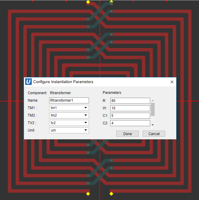
LTCC巴伦平面图
Top View of LTCC Baluns
LTCC巴伦3D图
3D View of LTCC Baluns
LTCC巴伦S参数图
S-Parameters of LTCC Baluns
LTCC 巴伦性能
Specifications
1.单元大小:1.9mm×1.7mm×177μm
2.通带:1.4GHz-5.18GHz
3.插入损耗:1.45dB
4.回波损耗: 11.3dB
5.相位不平衡度:7.85°
6.幅度不平衡度:0.46dB
7.共模抑制比:23dB
1.Dimensions:1.9mm×1.7mm×177μm
2.Pass Band:1.4GHz-5.18GHz
3.Insertion Loss:1.45dB
4.Return Loss: 11.3dB
5.Phase Imbalance:7.85°
6.Amplitude Imbalance:0.46dB
7.Common-Mode Rejection Ratio:23dB
AiP天线单元平面图
Top View of AiP Antennas
AiP天线单元3D图
3D View of AiP Antennas
AiP天线单元S参数图
S-Parameters of AiP Antennas
AiP 单元性能
Specifications
1.单元大小:5mm×5mm×632μm
2.隔离度:29dB
3.-10dB带宽:3.31GHz
4.交叉极化:<-13dB
5.大角度扫描:±60°
1.Dimensions:5mm×5mm×632μm
2.Isolation:29dB
3.-10dB Bandwidth:3.31GHz
4.Cross-Polarization: <-13dB
5.Large Scanning Angle: ±60°


PDK设计服务介绍
Introduction
我司拥有丰富的电子器件设计和EDA软件使用经验,又具有计算机软件开发经验,熟悉掌握行业常用电子设计软件及其集成架构,可针对不同工艺和不同EDA软件开发专用的PDK套件,便于用户进行芯片设计。
We have rich experience in EDA, both software development and tool usage. In particular, we have built up extensive experience in architecture and integration of industry's mainstream EDA tools. Furthermore, we have strong experience in developing PDK kits for various fabrication processes and different EDA tools.
PDK设计服务主要内容
Capabilities
1.参数化单元库(PCELL)创建:根据不同EDA工具的语法格式,对任意版图结构生成对应的参数化单元库,该库可以根据客户需求自由定制参数类型。
1.Parametrized Cell (PCell or FCell) Library Creation: For any given layout, we can create parameterized cell library according to customer's requirements.
2.工艺文件(Technology File)生成:根据工艺的叠层、材料等信息,生成各类仿真软件的工艺文件,便于客户直接导入仿真软件中使用。
2.Technology File Generation: According to stack, material and/or related geometrical/physical data of a given fabrication process, we can generate technology files for various EDA simulation tools.
3.SPICE等效电路建模:对PCELL或其它库单元进行等效电路建模,根据仿真或测试数据对电路模型进行拟合,生成准确的等效电路模型方便客户直接调用。
3.SPICE Equivalent Circuit Modeling: Based on the geometrical data of PCell, FCell or other layout cells, we can use our proprietary in-house full-wave EM simulator to generate accuracy EM data, and then create accurate equivalent circuit models for use in SPICE-type circuit simulators.
4.版图检查:根据工艺规则,生成DRC和LVS脚本文件,支持主流软件或定制化的文件格式。
4.Layout Check: According to the process rules, we can generate DRC and LVS script files to support various mainstream EDA tools or in a customized format.
设计自动化服务
Outsource Services: Design Flow
我司拥有电子设计专业的知识背景,又具有计算机软件开发经验,熟悉掌握行业常用电子设计软件及其集成架构,可解决设计工程师在版图设计中常常遇到的繁琐而极易出错的问题,加快设计速度、缩短设计周期,提高设计准确度。
We have strong professional knowledge and background in both electronic designs and software developments. In particular, we have built up extensive experience in architecture and integration of industry's mainstream EDA tools. We can tightly and seamlessly integrate various EDA tools to resolve the tedious and error-prone problems that are often encountered by design engineers, as well as further accelerate the design process, shorten the design cycle, and improve the design accuracy.
常见三类场景如下:
Typical scenarios:
1.建模类(Create):根据工程师日常设计中费时费力的场景,通过在设计软件上集成“一健式”设置,让设计工程师工作更便捷,提高设计自动化程度。
1.Modeling (Create): To make the designer's daily life easier, we can implement and integrate a "one-key" setup in the EDA tools to accomplish otherwise time-consuming and laborious jobs with a simple "pushing a button".
2.规则检查类(Report):设计中会有许多的规则检查,保证复杂设计的准确性,提高成品率,我司开发的自动化软件模块可准确快速完成检查,助力工程师定位问题,解决问题。
2.Rule Check (Report): Many rule checks are mandatory during design processes to ensure the accuracy of complex designs and improve the yield rate. The automation software modules developed by our company can accurately and quickly complete the rule checks to help the engineers identify and solve the potential problems.
3.输出类(Export):提取设计数据,导出文档,也是设计工作的重要一环,通过我司开发的自动化软件模块,减少人为干扰的失误率,提高设计工程师的工作效率。
3.Export: Extracting design data and exporting design documents are also an important part of design processes. Through the automation software modules developed by our company, one can greatly reduce human errors and improve work efficiency of the design engineers.
制图自动化服务
Outsource Services: Layout Generation
随着半导体行业的飞速发展,集成电路的尺寸微小性、电路复杂性带给制图工程师更多的困难与挑战,我司已与封装半导体头部企业建立制图自动化软件的开发合作,积累大量的制图自动化经验,致力解决人工核查造成误判等问题,提高制图审核效率,助力企业增效。目前,已打通市面常用国内外CAD工具的技术接口,实现图纸数据的自动化整理和分析,输出客户需要的DBS图纸。
With rapid advancement of the semiconductor industry, the chips become larger and more complex, which make the layout design designs much more challenges. We have extensive experience on interfaces of various CAD tools, realization of automatic sorting and analysis of drawing data, and generation of DBS drawings required by customers.